Designer Defects and Organic Charge Transport
Our group seeks to understand the fundamental properties of molecular electronic materials in order to produce new materials with higher charge mobility and conductivity, resulting in more efficient devices, including organic solar cells, light emitting diodes, flexible electronics, sensors, batteries, etc.
To do this, we combine experimental investigation of monolayer and nanoscale transistors with designed defects: both in terms of the type and concentration of defects. The combined experimental and computational research will enable greater understanding of charge transport in molecular materials.s
Experiment
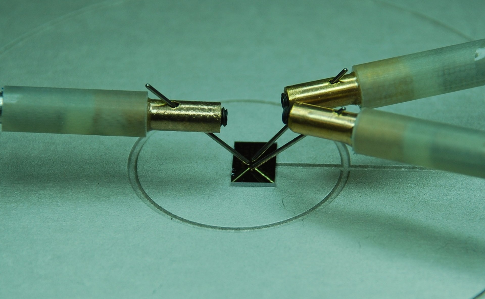 We synthesize a range of inorganic semiconducting complexes, such as metal phthalocyanines, as well as organic oligomers and polymers. We can tailor the relative electronic structure and concentrations of intentional designer defects. We fabricate our own chips and perform detailed device-level electrical characterization of the materials.
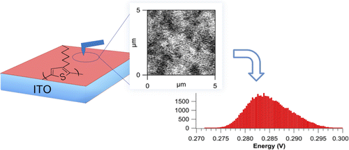
We also study nanoscale performance of devices using atomic force microscopy, including conductive-probe, electrostatic-force microscopy (local dielectric constant), and scanning-Kelvin probe microscopy.
Theory and Simulation
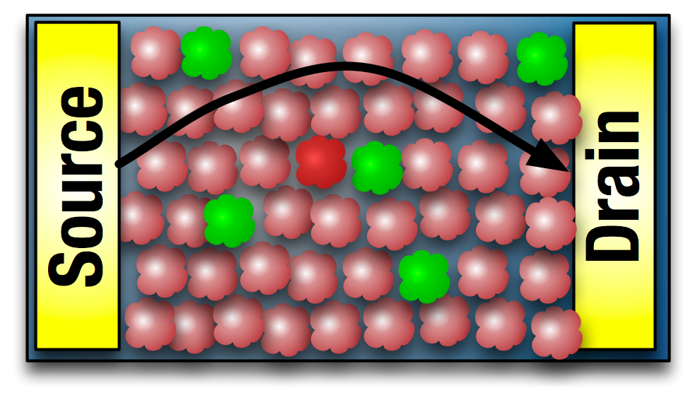 Our goal is to scale down our experimental transistors and scale up our simulations to provide a 1:1 correspondence between experiment and theory, benefiting both communities. So far, our code can easily handle micron-scale devices. We have demonstrated the exact distribution of charged and neutral defects in realistic transistors and the effect of Coulomb interactions on carrier trajectories. Results correlate extremely well with experiments.
In future work, we seek to use our combined approach to find materials with rapid charge transport for more efficient solar cells, transistors, light emitting diodes, and other applications.
Recent Publications:
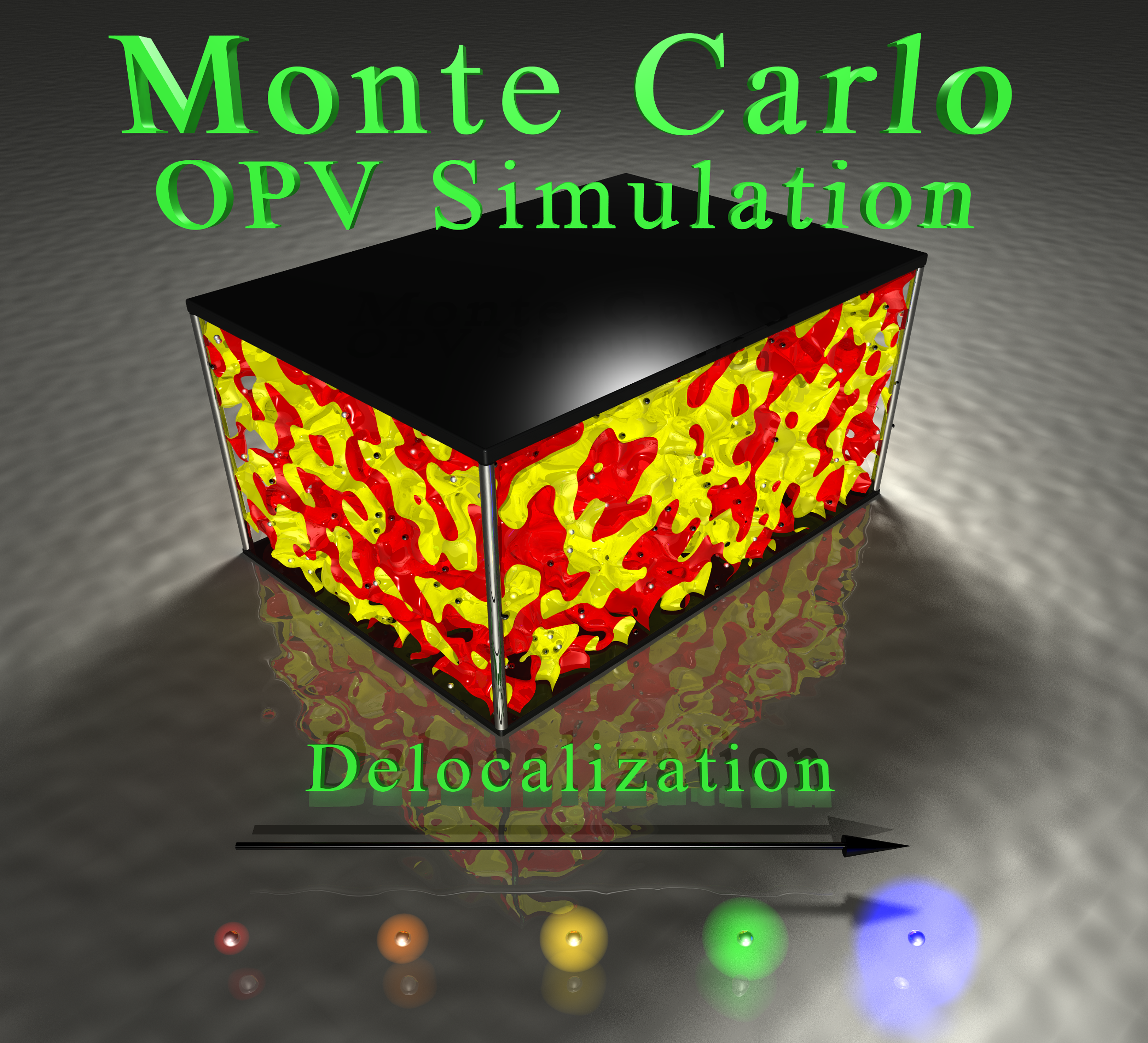
Effects of Delocalized Charge Carriers in Organic Solar Cells: Predicting Nanoscale Device Performance from Morphology
Adam G. Gagorik, Jacob W. Mohin, Tomasz Kowalewski and Geoffrey R. Hutchison “Asymmetric Surface Potential Energy Distributions in Organic Electronic Materia...
Asymmetric Surface Potential Energy Distributions in Organic Electronic Materials via KPFM
Paula B. Hoffmann, Adam G. Gagorik, Xialing Chen, and Geoffrey R. Hutchison. “Asymmetric Surface Potential Energy Distributions in Organic Electronic Materia...
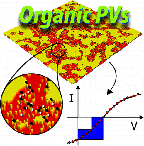
Monte Carlo Simulations of Charge Transport in 2D Organic Photovoltaics
Adam G. Gagorik, Jacob W. Mohin, Tomasz Kowalewski, and Geoffrey R. Hutchison. “Monte Carlo Simulations of Charge Transport in 2D Organic Photovoltaics” J. P...
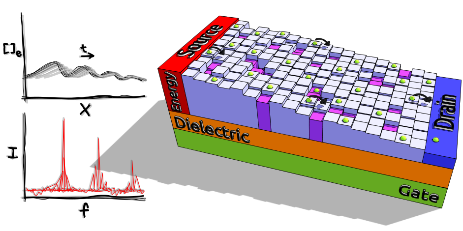
Simulating Charge Injection and Dynamics in Micro-scale Organic Field-Effect Transistors
Adam G. Gagorik, Geoffrey R. Hutchison. “Simulating Charge Injection and Dynamics in Micro-scale Organic Field-Effect Transistors” J. Phys. Chem. C 2012 116(...
